1. Introduction
At the nanoscale, which pertains to the atomic or molecular level, materials are purposefully designed and engineered in the realm of nanotechnology. This field allows for the development of innovative materials, tools, and systems that exhibit enhanced capabilities due to their manipulation of structures and particles at an extremely minute scale [1]. A nanoparticle is defined as a structure that experiences confinement in all three dimensions: x, y, and z. Conversely, when a structure is confined to only two dimensions, it takes the form of a nanowire or nanorod. Although a thin film has the ability to stretch over long distances in the x and y directions, its confinement remains limited to the z-direction. When it comes to analysis and characterization, particles are commonly treated as spheres or rods, despite their crystalline structure often leading to multifaceted shapes. Classification of structures can be based on the number of dimensions in which their size is restricted [2]. It could revolutionize a number of fields, including environmental science, electronics, medicine, and energy, providing answers to urgent problems and creating new opportunities for scientific research and technological development [3].
Semiconductors are substances with characteristics halfway between conductivity and insulativity [[4], [5], [6]]. As the basis for semiconductor devices like transistors, diodes, and integrated circuits, they are essential to modern electronics [7]. Semiconductors are crucial for the manipulation and processing of information in electronic devices because they have the capacity to control the flow of electrical current [8]. The electrical conductivity of semiconductors can be changed by doping them with impurities, which enables the development of sophisticated electronic components that power the modern digital world we live in Ref. [9]. Table 1 presents a summary of the characteristics exhibited by semiconductors.
Table 1. Material properties of semiconductors [10].
| Characteristics | Semiconductor |
|---|---|
| Conductivity | Moderate |
| Resistivity | Moderate |
| Forbidden gap | Small forbidden gap |
| Temperature Coefficient | Negative |
| Conduction | Very small number of electrons for conduction |
| Conductivity value | The conductivity of materials can range from 10^(-7) mho/m to 10^(-13) mho/m, distinguishing conductors from insulators |
| Resistivity value | Materials can have electrical conductivity ranging from 10^5 Ω-m to 10^5 Ω-m, classifying them as conductors or insulators |
| Current flow | Due to holes and unbound electrons |
| Number of carriers at normal temperature | Low |
| Zero Kelvin behavior | Acts like an insulator |
| Formation | Formed by covalent bonding |
| Valence electrons | The outermost shell contains a total of four valence electrons |
| Examples | Ge, Si, GaAs, GaP, CdS, InAs, InP, etc. |
Nanomaterials play a crucial role in enhancing energy conversion and storageapplications due to their unique properties, such as increased surface area and efficient mass [11], heat [12], and charge transfer [13]. In terms of energy applications, semiconductor nanoparticles have demonstrated promise in solar cells and harvesting industries [14]. To provide efficient and environmentally friendly alternatives to silicon-based solar cells, these materials can also be used to generate hydrogen [15]. Additionally, metal nanoparticles have the ability to substantially alter the optical characteristics of semiconductor nanoparticles [16]. Moreover, The Metal-Assisted Chemical Etching (MACE) technique involves utilizing metal nanoparticles to induce pore formation in silicon [17]. The Seebeck effect, which turns heat into electricity, is also demonstrated by semiconductor-based thermoelectric materials [18], and there are opportunities to improve performance by adding nanostructures and dopants [19]. Plethora of semiconducting nanoparticles showcasing advanced applications in Table 2.
Table 2. Semiconducting nanoparticles advanced applications.
| Semiconductors Nanoparticles | Size (nm) | Application | Year | Refs. |
|---|---|---|---|---|
| Fe2O3 | 2 to 10 | Hyperthermia for cancer treatment and the delivery of drugs | 2017 | [20] |
| Zinc Oxide, Titanium dioxide | More than 20 | Treatment of Dickeya dadantii in sweet potato | 2019 | [21] |
| Zinc Oxide | 53.7 | Nanoelectronics | 2011 | [22] |
| 57 to 72 | Treats Aspergillus flavus disease in maize | 2012 | [23] | |
| 28 to 84 | Treatment of Fusarium culmorum in Barley | 2013 | [24] | |
| 8 | Catalysis, drug delivery, biosensing, molecular diagnostics, cell labeling, solar cell technology, optoelectronics, and imaging | 2014 | [25] | |
| More than 41 | Treatment the disease caused by Xanthomonas oryzae pv. Oryzae | 2019 | [26] | |
| More than 66 | Treatment the disease caused by Xanthomonas oryzae pv. Oryzae | 2019 | [26] | |
| 2.72 | Antibacterial properties | 2020 | [27] | |
| Titanium dioxide | 12 to 15 | Fertilizer for plant nutrients | 2015 | [28] |
| Cupric Oxide | 78 to 80 | Treats Alternaria alternata, Fusarium oxysporum, Pythium ultimum, and Aspergillus niger in multiple crops | 2019 | [29] |
| Manganese dioxide and Magnesium oxide | 9 to 100 | Treatment of Acidovorax oryzae | 2019 | [30] |
| Magnesium oxide | Less than 20 | Treatment the disease caused by Xanthomonas oryzae pv. Oryzae | 2019 | [31] |
Nanoparticles' distinctive characteristics and uses add novelty to the semiconductor industry [32]. Nanoparticles provide improved functionalities and capabilities in semiconductor production due to their nanoscale dimensions. They are used as dopants for controlled electrical properties and in processes like chemical mechanical planarization for precise polishing [33]. Nanoparticles called quantum dots enable size-dependent emission and tunable bandgaps, revolutionizing optoelectronic devices and display technologies [34]. Nanoparticles are also used in printed electronics, which makes it possible to create flexible circuits [35]. Overall, nanoparticles open up new avenues for advancement and novel possibilities in semiconductor technology, improving performance and opening the door for further developments. Despite of so many advances, nanoparticles' potential impacts on the environment and the well-being of human beings must be carefully considered, and strong safety measures must be taken. To fully utilize nanoparticles in semiconductor applications and ensure their secure and long-term integration into future technologies, it will be essential to overcome these obstacles [36].
The goal of this review paper is to provide an overview of recent advancements in nanoparticle research and their applications in the semiconductor industry. The first part highlights the significance of nanoparticles as building blocks in various semiconductor devices and processes. The second part emphasizes the unique properties of nanoparticles that enable the introduction of novel functionalities and improved efficiency in semiconductors applications. The third part discussed the manufacturing processes of semiconductors in industrial level. The fourth and fifth parts analyzed NPs uses in semiconductors and semiconductors productions respectively. In final part, this paper acknowledges the challenges in synthesizing, integrating, and ensuring safety with nanoparticles. In conclusion, we need further research and development to overcome these obstacles and ensure successful implementation, recognizing the promising role of nanoparticles to shape the future of semiconductors applications.
2. Importance of semiconductor
Gadgets such as mobile phones, radios, televisions, computers, video games, and medical diagnostic apparatus, which are a vital aspect of our lives, rely on semiconductors for their functioning. Without semiconductors, these electronic devices would not be possible [37]. Semiconductor lasers with delayed feedback have proven to be well-suited for solving challenging and time-consuming tasks in photonic reservoir computing. In this technique, the reservoir is frequently optically injected with the input data [38]. Semiconductor helps electronics work by controlling the flow of electricity. In telecommunications equipment and systems, network and communication chips are semiconductor integrated circuits (IC) [39]. A variety of technologies are utilized in networking and communications chips, with a semiconductor material serving as the vital link between the conductor and the insulator. This material plays a crucial role in controlling and directing the flow of electricity within electronic devices and equipment. Consequently, it finds extensive application in electronic chips used for solid-state storage, computing components, and various other electronic devices [40]. As AI and machine learning enter and develop inside the banking industry, semiconductor chips assist banks even more. This wasn't a primary concern in the past because most attacks used software that was vulnerable to remote hacking [41,42].
Insulin pumps are now both wireless and tubeless thanks to semiconductors. Additionally, they include detection technology that enables insulin pump to pinpoint to precise moment at which our body requires additional insulin. Insulin pumps are now using polymer semiconductor [43].
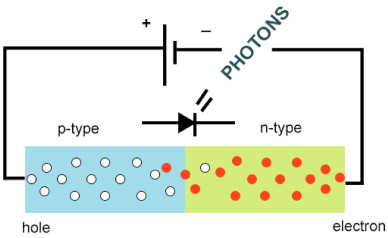
An LED, an acronym for light-emitting diode, operates as a semiconductor that facilitates the flow of electric current in a single direction. It is designed as a p-n junction diode, as depicted in Fig. 1, with an abundance of electrons residing in the n-type atoms and electron holes present in the p-type atoms. When an electric current is applied, it pushes the atoms towards the junction, causing the n-type and p-type atoms to come close together. Consequently, the excess electrons from the n-type atoms are transferred or “donated” to the p-type atoms, resulting in the accumulation of negative charge on the n-side. This accumulation initiates a current that moves from the negatively charged region to the positively charged region, known as “forward bias.” At the same time, as the extra electrons from the n-type material pass through the holes in the p-type material, they release energy in the form of light, known as photons [44]. LEDs demonstrate significant distinctions when compared to conventional light sources such a lamps, neon lamps, and gas discharge lamps. They possess the ability to illuminate swiftly, making them advantageous for battery-operated or energy-efficient devices. Moreover, LEDs generate a greater amount of light per Watt in comparison to incandescent bulbs [45] (see Fig. 2).
 Fig. 1. A circuit diagram of semiconductor chip [46].
 Fig. 2. Photocatalytic reaction mechanism [47].
With the introduction of semiconductors, automotive manufacturers now have the capability to utilize electronically controlled systems in place of manual ones [48]. Thanks to advancements in electrical systems, engineers have successfully developed automobiles that demonstrate improved efficiency, decreased reliance on oil, and reduced emissions of greenhouse gases. Semiconductor device fabrication, also referred to as the manufacturing processof semiconductor devices, involves the creation of integrated circuits (ICs) such as computer processors, microcontrollers, and memory chips like NAND flash and DRAM. These ICs are commonly found in various electrical and electronic devices [49]. It is also crucial to note that NPs exhibit distinct and frequently better physico-chemical properties than the corresponding bulk substance [50].
3. Advances of semiconductor applications
Semiconductor nanomaterials exhibit distinct properties and functionalities that set them apart from bulk and molecular materials, highlighting their unique characteristics. These include narrow emission spectra, continuous absorption bands, high stability, processability, and surface functionalities. The synthesis of semiconductor nanoparticles has seen significant advancements in the field of “nanochemistry” [51]. The spatial quantum confinement effect is responsible for notable alterations in the optical characteristics of semiconductor nanomaterials. These materials possess remarkable physical and chemical properties, coupled with a high degree of dispersity, making them subjects of extensive research and application in diverse fields. Electron and hole movement within these materials is influenced by quantum confinement, while the size and shape of the materials impact the transport properties of phonons (vibrational modes) and photons (light particles) [52].
In the 1960s, the initial semiconductor heterostructures were successfully synthesized, and they swiftly found applications in optoelectronic devices and fast-response electronics [53]. Subsequently, the development of nanostructures emerged, enabling the confinement of charge carriers in different dimensions. This confinement occurred in one dimension (quantum wells), two dimensions (quantum wires), and three dimensions (quantum dots), resulting in the quantization of energy states. The presence of a collection of nanostructures exhibits distinct properties related to transportation, electrical behavior, optical characteristics, absorption abilities, and other factors, which are intricately influenced by their size and shape. The need to precisely control the growth of nanostructures, with desired sizes, densities, and shapes, has become increasingly urgent due to the complex relationship between the physical properties of particles and their geometry [53].
In 1972, Fujishima and Honda made a significant discovery indicating that the presence of sunlight can trigger the decomposition of hydrogen in water when a TiO2 electrode is exposed to it [54]. Due to its direct conversion of solar energy to readily storable hydrogen and lack of environmental contamination, photocatalysis has since garnered a lot of attention.
A vast market for the internet and wireless communication was created at the start of the twenty-first century as semiconductor process technology advanced from the sub-micron generation to the nano-era and product design underwent revolutionary advancement. The semiconductor industry's technical innovation had an impact on both the demand for the product as well as the supply side (production and cost). The performance of semiconductor companies is now significantly influenced by technical innovation, which is also of interest to investors, particularly institutional investors. However, very few valuation studies have been conducted on the investment value of technical innovation, primarily due to the difficulty of measuring the performance (or capability) of technical innovation [55].
The composition and crystal structure of semiconductor materials allow for the engineering of optical properties [56]. Electrocatalysis is highly correlated with the type of semiconductor catalyst; specially, n-type catalysts favor cathodic reactions like the hydrogen evolution reaction, and bipolar catalyst typically carry out both anodic and cathodic reactions [57]. In solar energy conversion applications, and in-depth understanding of the photocatalytic mechanism for hollow semiconductor photocatalysts formation may offer fresh perspectives on how to create high-performance hollow photocatalysts [58].
The exceptional properties of semiconductor nanomaterials have garnered significant attention and enthusiasm in a multitude of advanced technologies. These include nanophotonics, nanoelectronics, miniaturized sensors, energy conversion, non-linear optics, detectors, imaging devices, quantum applications, solar cells, catalysis, photography, water treatment, and biomedicine.
3.1. Semiconductor application in energy
Nanomaterials offer significant advantages that play a critical role in improving energy conversion and storage applications. One key advantage is their ability to facilitate physical interactions or chemical reactions at the surface or interface, which greatly impacts their effectiveness. The specific surface area, surface energy, and surface chemistry are particularly important factors that strongly influence energy-related processes. These factors affect the kinetics and thermodynamics of reactions taking place at the interface, as well as the initiation and growth of phase transitions. Moreover, the smaller size of nanomaterials allows for more efficient transfer of mass, heat, and charge, while also accommodating dimensional changes that occur during certain chemical reactions and phase transitions. However, despite their numerous benefits, the integration of nanomaterials into energy conversion and storage systems presents unique challenges. For example, the large specific surface area can lead to increased charge recombination in photovoltaics [59], while the presence of smaller pores, especially micropores (<2 nm in diameter)may contributes the penetration of electrolyte ions in supercapacitors [60,61].
3.1.1. Hydrogen evolution reactions (HER)
Hydrogen, obtained through the photocatalytic splitting of water, offers a safe and environmentally friendly alternative energy source capable of mitigating the detrimental impacts of fossil fuels. This emerging technique utilizes photocatalysts to facilitate hydrogen production, harnessing the omnipresent resource of water while being activated by solar energy. The resultant catalysts yield eco-friendly by-products and are required to possess chemical stability, corrosion resistance, and the ability to absorb radiation within the visible spectrum for efficient energy generation [62]. The performance of transition metal dichalcogenides (TMDCs) as electrocatalysts for the hydrogen evolution reaction (HER) is hindered by limited active reaction sites and relatively low electrical conductivity. This applies to TMDCs such as MoS2 and WS2 [63].
3.1.2. Applications in solar cells
Semiconductor nanoparticles possess favorable qualities that present a promising substitute for silicon-based solar cells. These characteristics encompass affordability, an adjustable band gap, the capacity to generate multiple electron-hole pairs, a heightened optical absorption coefficient, and the quantum size effect. Among the diverse array of binary metal chalcogenides, such as PbS, PbSe, CdS, CdSe, and Ag2S, solar cells incorporating these materials have garnered considerable interest. This is primarily due to their ability to efficiently absorb light within the desirable band gap range of 1.1–1.4 eV [64].
3.1.3. Thermoelectric energy conversion
Semiconductors are essential in thermoelectric energy conversion, which uses the Seebeck effect to directly convert heat into electricity [65]. The Seebeck effect occurs in certain materials, including semiconductors, and causes a voltage to be generated across the material when a temperature gradient is applied to it [66]. This phenomenon enables the use of semiconductor-based thermoelectric materials in thermoelectric generators (TEGs) and thermoelectric coolers (TECs) [67]. TEGs work best with semiconductors that have good thermoelectric properties, such as high electrical conductivity and low thermal conductivity [68]. In order to boost the thermoelectric performance and increase the efficiency of the conversion of heat into electricity, researchers frequently use materials with intricate nanostructures or add dopants [69]. On the other hand, high thermoelectric efficiency semiconductor materials are preferred for thermoelectric cooling applications [70]. Electrical, thermal, and figure of merit of the semiconductor material are just a few examples of the variables that affect how well TECs cool [71]. Better thermoelectric performance is indicated by a higher ZT value [72].
3.1.4. Energy storage
Semiconductors, unlike batteries and capacitors, are not directly used for energy storage [73]. Instead, they are utilized in energy conversion procedures that are sometimes connected to energy storage [74]. Their contribution to grid integration and energy conversion technologies is essential for efficiently utilizing and managing energy storage systems [75]. Semiconductors help maximize the effectiveness of energy storage solutions and contribute to a more dependable and sustainable energy infrastructure by enabling efficient energy conversion [76].
3.2. Quantum applications
When it comes to quantum applications, semiconductor qubits are incredibly adaptable and cover a complete ecosystem. This is especially true when considering quantum simulation, sensing, computation, and communication [77]. For practical applications in sustainable reuse, a photocatalyst's stability is crucial. The stability and repeatability of semiconductor-based catalysts are typically explored by the use of recycle experiments, in which the photocatalysts are gathered and repeatedly employed for specific photocatalytic reactions [78]. Industries involved in the production of semiconductor integrated circuits employ intricate procedures such as wire bonding, wafer back grinding, sawing, die attachment, trimming, encapsulation, electroplating, forming, and marking [79]. Samsung Electronics overtakes Intel as the leading manufacturer of semiconductor chips with sales of 75.85 billion US dollars whereas, Intel remained in 69.8 billion US dollar sales income. As of right now, semiconductor technology has integrated 100.8 million transistors at a node size of under 10 nm [80].
3.3. Water treatment
Photocatalytic water splitting presents an alternative strategy for tackling resource and environmental challenges, offering a hopeful avenue for producing clean and sustainable energy. The emergence of novel catalysts utilizing semiconductor nanoparticles has garnered growing interest due to their ability to facilitate all the necessary reactions for achieving “artificial photosynthesis” [81]. The subsequent successful oxidation of CN to OCN by Frank and Bard using TiO2 as a photocatalyst encouraged and accelerated the use of photocatalysts in wastewater treatment [82]. Researchers have written numerous great assessments as photocatalytic technology continues to advance. For instance, Wang et al. discussed how nitrogen doping can be used to change oxide photocatalysts in order to enhance their photocatalytic performance [83]. When a photocatalyst and light collaborate, they give rise to a chemical process referred to as a photocatalytic reaction. This particular approach boasts numerous advantages, such as the absence of secondary pollution, complete degradation of pollutants, and the promotion of environmental preservation [[84], [85], [86], [87], [88]].
3.4. Semiconductor application in biomedical
In recent years, 2D nanomaterials beyond graphene (2D NBG) have emerged as a fascinating class of materials with exceptional antibacterial properties, surpassing even the renowned graphene. These nanomaterials comprise a diverse range of compounds, including Two-dimensional transition metal dichalcogenides (TMDCs), g-C3N4, transition metallic oxides (CaO, MgO, etc.), black phosphorus (BP), layered double hydroxides (LDHs), and transition metal carbides and nitrides. Their effectiveness in various biomedical applications, such as anticancer, antimicrobial, and antiviral treatments, has garnered significant attention. The key factors influencing their performance in these applications include size, morphology, crystal orientation, concentration in the growth medium, stability, and surface functionalization [89,90]. Given these unique attributes, 2D NBG nanomaterials hold tremendous promise as cutting-edge tools for advancing biomedical research and healthcare technologies.
3.4.1. Antibacterial agents
By employing a non-invasive and targeted approach, the photoinduced antibacterial mechanism demonstrates a treatment method with minimal to no adverse effects. This method involves the activation of photoresponsive semiconductors upon exposure to light energy, leading to the stimulation of fluorophores. Consequently, these fluorophores are transformed into either heat or reactive oxygen species (ROS), which effectively combat bacterial organisms. Within this context, MoS2 nanosheets exhibit remarkable photothermal efficiency in the near infra-red range, making them highly promising agents for photothermal antibacterial purposes [89]. By subjecting ZnO and TiO2 nanoparticles to ultraviolet radiation, pathogenic bacteria can be destroyed [91]. Their safety and multifunctionality have led to their recognition as antimicrobial agents suitable for various applications. Due to their biocompatible properties, nanoparticles have demonstrated utility not only in the realm of drugs and pharmaceuticals but also in various other fields such as cosmetics, food packaging, and wound healing [92].
3.4.2. Anticancer behavior
The nonspecificity of drug action in cancer chemotherapy is increasingly posing challenges due to the occurrence of transformational or decompositional behaviors during the transportation of metal-based drugs into the cell membrane [93]. Developed are non-classical metallodrug-functionalized nanostructures, which demonstrate diverse mechanisms for damaging cell DNA and inducing tumor cell death. Among the essential semiconductor nanoparticles for cancer diagnosis and therapy, iron oxide nanoparticles (IONPs) hold significant importance. They possess multifunctional properties, primarily attributed to their magnetic and harmless characteristics, biocompatibility, stability, and affordability [94]. Selective drug delivery, magnetic resonance imaging (MRI), magnetic separation techniques, magnetic fluid hyperthermia and thermoablation, as well as biosensing methods are among the various biomedical applications of IONPs [95].
3.5. Semiconductor application in sensing
Effective monitoring and control are indispensable for a wide range of natural and human endeavors. These encompass diverse activities such as forest fires, explosives handling, petroleum and metal refining, mining waste management, vehicle emissions control, natural gas utilization, plastic waste management, coal utilization, the combustion of fossil fuels, and the production processes involved in both food and industrial manufacturing [96]. These activities, which play a vital role in our daily lives, unfortunately also generate substantial quantities of pollutants. Additionally, it is important to note that volcanoes also contribute to this environmental pollution [96]. Environmental concerns have made sensing an essential component of environmental studies, enabling the detection of hazards in our surroundings. Essentially, a sensor is an electronically fabricated device that exhibits surface changes upon stimulation by chemical agents [97]. Detection and monitoring of hazardous chemicals, noxious gases, gas detection systems, temperature variations, water and soil contaminants, and the well-being of individuals, can be achieved through the use of chemical sensors.
Semiconducting metal oxide sensors, including ZnO [98], SnO2 [99], WO3 [100], CuO [101,102], Fe2O3 [103], In2O3 [104,105], CdO [106], TeO2 [107], and MoO3[108], have been widely employed among the various gas sensor options. Zinc oxide nanostructures with various shapes and structures have been extensively researched and utilized in the field of gas sensing applications, such as nanorods [[109], [110], [111], [112], [113], [114], [115], [116], [117], [118]], nanowires [119,120], nanofibers [121], nanolines [122], nanobelts [123], nanoneedles [124], nanoprism [125], nanotubes [126], nano/microflowers [127,128], quantum dots [[129], [130], [131]], nanoparticles [[132], [133], [134]], nanofilms, sheets, and plates [[135], [136], [137]], nano/microspheres [138], nanopyramids [139], and nanotetrapods [140]. These substances exhibit notable characteristics such as elevated electron mobility, a lack of toxicity, a large surface area per unit mass, and exceptional stability in both chemical and thermal environments [141,142] under operating conditions.
3.6. Semiconductor application in electronics
Semiconductors possess easily regulated properties, rendering them highly valuable in the realm of electronics. Their ubiquitous presence extends to a wide array of commercial products, spanning from family cars to pocket calculators. The extensive utilization of semiconductor devices encompasses diverse industries, including computers production, communications, aerospace, manufacturing, agriculture, and healthcare. By enabling more compact, cost-effective, rapid, and more reliable electronic devices such as music players, LED TV, DVD players, laptops, and mobile phones, semiconductors have revolutionized the field. Additionally, semiconductors play a pivotal role in scientific research and industrial operations [143].
4. Semiconductor manufacturing process
One of the biggest industries in the world now is the electronics sector. The production of integrated circuits is a crucial component of this sector. On silicon wafers, integrated circuits are manufactured in the semiconductor industry. Historically, cost-cutting measures have included shrinking chip size, expanding wafer size, and raising yield while also attempting to enhance operating procedures inside semiconductor manufacturing systems [144]. Integrated circuit (IC) usage has been rising quickly and will probably keep doing so in the near future. As a result, the production of semiconductors remains a hot topic in the world of manufacturing [145].
Chemical mechanical polishing (CMP) is a crucial planarization step in the production of semiconductors. CMP is being used more frequently in the manufacture of semiconductors for devices with a high level of integration. Recently, the environmental impact of the CMP process was evaluated due to interest in the environment worldwide [146]. Chemical mechanical polishing (CMP) removes material by combining mechanical and chemical forces [147,148]. When compared to other planarization techniques, CMP has the greatest planarization length, which makes it crucial for device production even if it contains particles that can kill by deflecting or scratching. The surface of the chemically softened material is mechanically removed is the primary working principle of the CMP process [149,150]. Three words best describe the future of CMP technology: growth, digitization, and sustainability. Starting with highly integrated circuits, 3D microelectromechanical systems (MEMS), fan-out panel level packaging (FOPLP), and substrates that are free from defects, its use is becoming more and more diverse. In the near future, CMP will be able to remove more than 40 different types of materials and develop solutions for every type of substance. Additionally, the electrochemical processes within the CMP (Chemical Mechanical Polishing) technology are anticipated to be used not only in the traditional domains of semiconductors and displays, but also in others like maskless electrochemical texturing [151,152].
The move from 200 mm to 300 mm wafers has begun in the semiconductor industry in an effort to increase manufacturing productivity and lower manufacturing costs [153]. As wafers move through a wafer fabrication facility (fab), a considerable amount of data is automatically generated. This data encompasses a wide range of valuable information, including details about the manufacturing processes, historical data for each lot, tool profiles, and the outcomes of wafer acceptance tests. Semiconductor manufacturing is very complex and consists of hundreds of process steps [154]. Fig. 3 shows us those important steps.
 Fig. 3. Steps ofsemiconductor manufacturing.