1. Introduction
Aluminum nitride (AlN) is a semiconductor with a wide band-gap (5.8 eV) [1] and high resistivity (~1012 Ohm·cm) [2], breakdown field (>1.2 × 10⁶ V.cm−1) [3], thermal conductivity (162 W.m−1.K−1) [4] and acoustic velocity (~11.000 m.s−1) [4]. Because of its satisfactory effective electromechanical coupling coefficient (keff ~ 0.23 [5]), which is comparable to that of other piezoelectric materials such as ZnO (keff ~ 0.28 [6]) or LiNbO3 (keff ~ 0.24 [7]), AlN has been used in several commercial applications, mainly in film bulk acoustic resonators (FBAR) and surface acoustic wave (SAW) resonators for RF filters, in the telecommunications sector [8]. Recent emerging applications of AlN include optoelectronics/photonics [9,10], sensing [11] and energy harvesting [12,13].
AlN is a wurtzite-structured material (hexagonal symmetry) that can be deposited as a thin-film for application in microelectromechanical systems(MEMS). Physical vapor deposition by reactive magnetron sputtering is the most commonly used technique as it allows the low-temperature deposition of well-oriented polycrystalline piezoelectric AlN films [3,14,15]. Such thin-films are usually c-axis, out-of-plane oriented (0002), and their crystalline properties can be assessed by x-ray diffraction (XRD). The low temperature deposition guarantees process compatibility with a wide range of materials and with most complementary metal oxide semiconductor (CMOS) devices, which only tolerate temperatures below 450 °C (in sub-100 nm processes, higher temperatures may lead to dopant diffusion and poor performance) [16]. Contrary to lead zirconate titanate (PZT), AlN does not introduce lead contamination on the cleanroom process equipment or the environment, and it does not require a post-deposition poling step. However, because AlN is not ferroelectric, the polarization of the material cannot be changed after deposition and as such it should be grown with the desired crystalline orientation, usually c-axis, (0002)-oriented. Recently, it was shown that the piezoelectric properties of AlN can be improved by doping it with certain elements such as scandium (Sc). Scandium Aluminum Nitride (ScxAl1-xN), prepared by co-sputtering, exhibits enhanced piezoelectric coefficients ~500% larger than those of AlN [17].
For the fabrication of piezoelectric MEMS devices based on AlN thin-films, the deposition of the material with the correct orientation and appropriate physicochemical properties is not sufficient on its own, i.e., the AlN film must be patterned in order to define a particular shape. After film deposition, patterning is achieved by performing a lithographic step on a photosensitive material (photoresist), which protects part of AlN layer (depending on the design) while exposing the remaining material for selective removal (etching). Different wet etching chemistries and dry/plasma etching methods can result in distinct etch patterns (isotropic vs anisotropic etch profile) and material selectivity. Essentially, wet and dry etching techniques can be complementary, but depending on the requirements and tolerances of the device to be fabricated, one technique may be preferred over the others.
Wet etching occurs due to chemical reactions that convert the thin solid film into soluble by-products that dissolve in the liquid solution and allow the selective removal of the material. Wet etch is known to be isotropic, but that may not apply in materials with well-defined crystalline orientations (including thin-films). Wet etching can exhibit good selectivity over other materials. On the contrary, dry etching techniques are usually highly anisotropic and less selective. Dry etching, such as ion milling or reactive ion etching (RIE), can produce vertical profiles, but may induce damage due to ion bombardmenteffects or induce hydrogen contamination on the AlN film, changing its conductivity [18]. Wet etching does not cause damage by ion bombardment effects, avoids hydrogen incorporation and is easy to implement in an inexpensive manner.
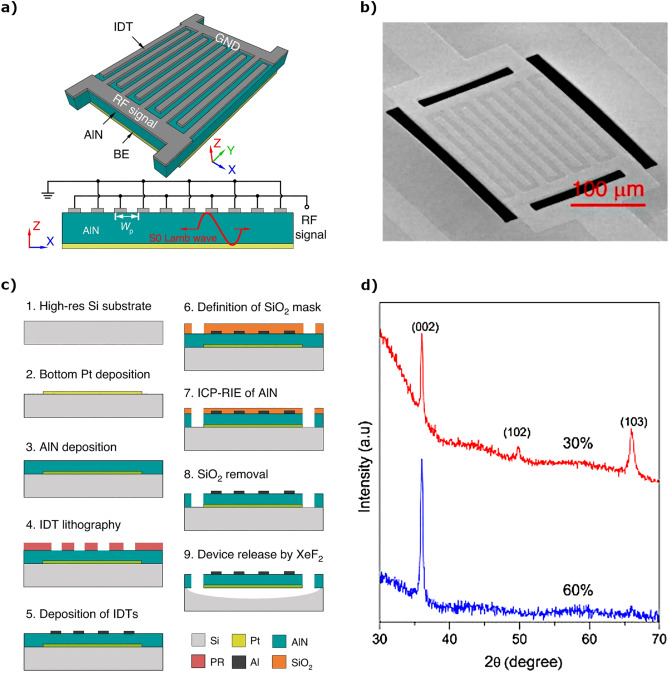
An example of a MEMS device that requires patterning and etching of an AlN layer is depicted in Fig. 1: a Lamb wave resonator used in RF filters. The simplified geometry and the final device can be appreciated in Fig. 1, a), and b), respectively. The fabrication, illustrated in Fig. 1, c), starts with the deposition and patterning of a bottom electrode on top of a Si substrate, followed by the deposition of the piezoelectric AlN layer and deposition and patterning (by lift-off) of the top interdigitated (IDT) electrodes. A SiO2 hard mask is used to define the shape of the AlN layer, instead of photoresist (PR), due to the considerable thickness of the piezoelectric layer (1 μm). Finally, the AlN piezoelectric layer is etched by inductively-coupled plasma reactive ion etching (ICP-RIE), the hard mask is removed with HF and the device is released by etching the Si underneath the resonator, using a XeF2 dry vapor etch [19].
 Fig. 1. a) Schematic representation of an AlN Lamb wave MEMS resonator. The resonator consists of three layers: bottom electrode, AlN thin-film, and top IDT electrodes. b) Scanning electron microscopy image of the actual device. c) Cross-section representation of the fabrication process, which involved the anisotropic etch of the AlN layer by ICP-RIE and the isotropic (dry) etch of the underlying silicon for resonator release (XeF2). Fig. 1 a), b) and c) are reproduced from [19] under the terms of the Creative Commons Attribution 4.0 license (CC BY 4.0). d) XRD Bragg-Brentano scan of two AlN thin-films deposited by reactive magnetron sputtering using two different plasma compositions (the nitrogen flow fraction was 30% and 60%, respectively). Reprinted from [20] under the terms of the Creative Commons Attribution 4.0 license (CC BY-NC-ND 4.0).
Two examples of XRD scans of AlN thin-films deposited using different conditions are provided in Fig. 1, d). The predominant crystalline orientations can be identified in a Bragg-Brentano scan (θ scan), while the dispersion around a certain orientation can be assessed by the full-width at half maximum (FWHM) of a rocking curve (ω scan) performed around a particular θ angle.
An alternative to etching processes is lift-off. In this case, the lithography is performed prior to film deposition, to define a photoresist layer with openings where the deposited material should remain. Then, the film is deposited and the photoresist mask is selectively removed with an appropriate solvent, resulting in the “lift-off” of the material that was deposited on top of the photoresist. The main limitations of lift-off are the thin-film deposition temperature, which must remain below ~150 °C (to avoid the degradation of the photoresist polymer or excessive hardening), the film thickness that can be deposited without hindering the lift-off process (limited by the photoresist thickness and the undercut profile), and the fact that it is a wet process. For example, highly c-axis oriented AlN has been deposited at low temperatures using a tilt gun DC sputtering method, allowing the patterning of cantilever resonators using lift-off [21]. Other examples of room temperature AlN deposition or without intentional substrate heating can be found in the literature [[22], [23], [24]], which indicates that although not very common, in some cases lift-off can be suited for AlN patterning. Consequently, this review focuses on the mainstream etching processes.
Given the technological importance of AlN and the multitude of applications that require the patterning of the material, a review on the topic is timely. The main objective of this paper is to compile and discuss the different wet and dry etching methods for AlN reported to date, facilitating and speeding up the implementation of the material in a variety of MEMS processes. The review is organized as follows. Section 2 discusses the importance of AlN polarity and crystallinity in the wet etch process, and then introduces the acid and alkaline wet etch approaches. Section 3 reviews ion beam etching (IBE), reactive ion beam etching (RIBE), reactive ion etching (RIE) and ICP-RIE dry-etch techniques available for the patterning of AlN. The etching mechanisms and chemical reactions are introduced in each case. Section 4 closes the review with the most important conclusions regarding each type of process and highlights future development needs.
2. Wet etching
Group III nitrides, such as AlN and GaN, are notable for their excellent chemical stability, nevertheless some possibilities for chemical wet etching exist, including aqueous mineral acid and base solutions, or molten salts. However, etching parameters depend on the crystalline quality and properties of the AlN film [18]. Compared to epitaxial films, polycrystalline AlN films are more vulnerable to wet etch with hot phosphoric acid (H3PO4), hot HF/H2O, HF/HNO3and NaOH solutions, with low-crystallinity films being more prone to higher etch rates [18].
2.1. The influence of polarity and crystallinity in the AlN etch process
The wurtzite structure of AlN consists of alternating layers of Al N pairs, stacked along the c-axis direction in an Al-N-Al-N-Al-N sequence, thus the basal plane can be either N- or Al- polar, as depicted in Fig. 2. Film polarity can be identified after wet etching since the etch rate and the resulting surface morphology is polarity-dependent [18,25]. In general, a polycrystalline film can have a mixture of the two polarities, resulting in a degradation of the net piezoelectric response, thus the occurrence of inversion domains must be minimized if a high-quality piezoelectric AlN thin-film is desired [26].
 Fig. 2. Polarity of the AlN: Al-polar (a) vs N-polar. Reprinted from [27] under the terms of the Creative Commons Attribution 4.0 license (CC BY 4.0).
Most AlN-based piezoelectric devices have been grown on the Al-polar face since this polar orientation is characterized by low impurity incorporation and a fully coalesced film with smooth surface and few defects. In contrast, N-polar films exhibit a columnar structure that is coalesced near the bottom and display a rougher surface [25].
2.2. Acid solutions
The general hydrolysis reaction of AlN, which can lead to its dissolution in aqueous media, has been proposed to be mediated by the following mechanisms: [28].(1)(2)(3)
In the hydrolysis process, first an amorphous AlOOH layer is formed and dissolved in water (Reaction 1), forming different aluminum species which are eventually (Reaction 3) precipitated as bayerite (Al(OH)3) [29]. When studying the reactivity of AlN (in powder form) with different acid solutions (HCl, HF, HNO3, H2SO4, H2CO3 and H3PO4) it was concluded that at pH < 1 no reaction occurs, regardless of the acid used. At pH >3, monoprotonic acids (which are completely dissociated) form water-soluble salts with aluminum, and for incompletely dissociated diprotonic acids the reaction was hindered but not prevented [29]. In the presence of phosphoric acid the hydrolysis was prevented at room temperature, likely due to the formation of insoluble phosphates on the surface of the material, but at elevated temperatures the reactivity was re-established and the solubility was substantial [29]. Consequently, the use of high temperature during the wet etch of AlN thin-films in phosphoric acid solutions is favorable.
In high c-axis AlN thin-films, deposited by magnetron sputtering at room temperature, the use of 85% H3PO4 at 80 °C results in etch rates of ~300 nm/min [30]. The etch rates depend on the phases which are present in the AlN film and a low etch rate has been associated with a predominant c-axis orientation (densely-packed film) [30]. Additionally, the etched surface typically shows an increased roughness with the formation of conic structures during phosphoric acid etch, due to the slow etching of the {012} planes [31].
After the sputter deposition of AlN on a Mo seed layer, phosphoric acid solutions were used to test the ability to completely etch the film (43% H3PO4heated to 90 °C) or to reveal the structure of the film (12.5% H3PO4 heated to 90 °C) [26]. Some films are etch-resistant, developing conical structures presenting a face of the AlN crystal structure that is chemically stable in hot phosphoric acid, stopping the etch process. Etch resistant AlN films have a larger columnar grain structure and develop protrusions at the surface (Fig. 3(a)), which can be attributed to the existence of stacking faults and inversion domains in the AlN film, although the later could not be experimentally confirmed in this work [26]. On the contrary, films that are easily etched display a fine grain structure in the early stages of film growth, which then evolve into a columnar structure [26]. The use of a Mo underlayer with higher roughness resulted in an increase of the FWHM of the AlN XRD rocking curve (degradation of the crystalline quality) and lead to the development of conical features on the surface of the AlN, which hints at an increased occurrence of inversion domains in the AlN film [26]. The use of a RF plasma etch of the Mo surface prior to the AlN deposition influences the ability to etch the AlN, as films deposited without the use of a sputter etch are not completely removed in the phosphoric acid. In contrast, the use of a 30 s low-power etch greatly reduces the occurrence of structures that cannot be completely etched/removed [26]. Increasing the RF power or time of the plasma etch beyond this optimal point leads to the formation of whiskers at the surface of the bottom electrode and an increase in the occurrence of inversion domains in the AlN film [26].
 Fig. 3. Patterning of AlN using wet etching techniques. a) Cross-section SEM micrograph of Mo/AlN thin-films (300/1000 nm) after a 10 s etching in 12.5% H3PO4 at a temperature of 90 °C. Formation of conical structures at the surface of AlN thin films occurs in etch-resistant films and are associated to the existence of stacking faults and inversion domains in such AlN films. Reprinted from [26] with permission from the American Vacuum Society. b) Tilted SEM micrograph of a Cr/AlN/Cr structure after AlN wet etching with a TMAH solution (25 wt%). The anisotropic pattern is visible (minimal undercut below the Cr top electrode/mask). Reprinted from [32] with the permission from Elsevier.
It was also demonstrated that the c-axis oriented AlN thin-film wet etch in phosphoric acid (H3PO4) is, in general, anisotropic. When using a 85% H3PO4solution at 80 °C the etch rate in the direction perpendicular to the wafer surface (c-axis) is only 2.6–3.7 nm/s but in the direction parallel to the surface it is up to 12 nm/s, developing pronounced undercuts [33].
When fabricating AlN/GaN metal insulator semiconductor field effect transistor(MISFET) devices, the selectivity of the AlN wet etch with phosphoric acid was investigated [34]. For AlN and GaN films deposited by radio-frequency plasma-assisted molecular beam epitaxy, the phosphoric acid etch of AlN occurred for temperatures above 160 °C while GaN films were etched only above 210 °C. Thus, in this process the AlN material was etched selectively at 170 °C with characteristic etch rates in the range 7–10 nm/min [34].
The wet etch with phosphoric acid solutions allows the use of a standard photoresist etch mask, which can then be removed with typical resist removers (Arch Chemicals RER500 or Du Pont EKC830) without damaging the AlN layer or producing pinholes [35]. Metal mask layers of titanium or chromium can also be used for pattern definition and then removed with buffered oxide etch (BOE) or cerium (IV) ammonium nitrate (CAN), respectively, without damaging AlN, as the nitride layer is not significantly attacked by these etchant solutions [35].
2.3. Alkaline solutions
One of the most common basic solutions for the wet etch of AlN is potassiumhydroxide (KOH). The typical etch rate of a c-axis oriented AlN thin-film using a 15% KOH solution at room temperature is ~50 Å/s [30]. The KOH wet etch has been proposed to be governed by the following reaction: [18].(4)
A common photoresist developer, AZ400K (contains KOH with concentrations ranging 2–5% [36]), has also been verified to etch AlN thin-films resulting in typical etch rates of ~0.7 nm/s in the c-axis direction [33]. The effects of AZ400K on polycrystalline AlN have been further studied using pure and diluted (5:1 H2O:AZ400K) solutions [37]. The etch profile of the AlN layer was found to be temperature-dependent: very little undercut was produced at 65 °C, while at 85 °C a substantial undercut was produced [37]. A good control of the undercut formed by wet etching is a requirement for the fabrication of a variety of devices. Furthermore, the authors have concluded that the etch of AlN films with AZ400K does not depend on the crystallographic orientation and is selective over GaN, InN, Al2O3 and GaAs [37].
These simple and low-cost wet etching techniques can also be used to reveal defects by selecting an appropriate set of etchants and conditions so that the local etch rate at a defect is different from that of the bulk of the material – at the defect, the composition and/or physical structure is different. Examples of defects that are visible after etching include etch pits or hillocks on a semiconductor surface [18]. The formation of hillocks at the surface of the substrate after the etching of AlN thin-films with KOH can be explained by the existence of distinct etch rates for the different crystallographic planes. When studying the etch of AlN single crystals in a KOH solution (45 wt%, at 60 °C), it was verified that the N-polar (0001) basal plane initially etched rapidly, while the Al-polar basal plane and the prismatic (1100) planes were not etched, resulting in a surface covered with hexagonal hillocks [38]. The N-polar surface of high-quality AlN bulk crystals have typical etch rates of 1400 nm/min while the Al-polar surface etches at a rate of ~2 nm/min, thus, it can be concluded that an Al-polar surface is more inert to the KOH etch [39].
An alternative to KOH for the AlN wet etch is tetra methyl ammonium hydroxide (TMAH). Very high etch rates (8000 nm/min) have been measured when using TMAH (25 wt%) heated at 82 °C, demonstrating its suitability for the etching of thicker films. For comparison, a phosphoric acid based solution (80% H3PO4, 16% H2O and 4% HNO3) at 90 °C showed a much lower etch rate (90 nm/min) [31].
An example of a simple but effective microfabrication process employing wet etching can be found in [32], where piezoelectric-actuated devices were fabricated from a stack of Cr/AlN/Cr layers deposited without breaking the vacuum and then patterned using a wet etch process. The top Cr layer serves simultaneously as an etch mask and as a top electrode. The anisotropic etch of the columnar AlN thin-film was performed with a TMAH solution (25 wt%, at room temperature), resulting in a vertical etch rate of 22 nm/min and negligible lateral etching under the Cr mask (<2 nm/min), as depicted in Fig. 3(b) [32].
For the benefit of the process developer, Table 1 contains the etch rates for the different wet etching solutions discussed in the text, as a function of the chemistry, concentration and temperature. The selectivity of the etch is also indicated – for example, if a PR mask was used, we assume the etch is selective against PR, that is, the etch rate of the etching mask is significantly lower than that of the material under study (AlN). However, the wet etch with any of these solutions may be selective against other materials not indicated in the referenced studies.
Table 1. Wet etching solutions for AlN polycrystalline films (unless otherwise stated) and corresponding etch rates as a function of the chemistry, concentration and temperature. The selectivity of the etch process is also indicated as far as is can be deduced from the reading of the referenced articles (materials not etched or etched at a much lower rate than AlN).
| Aqueous Etchant Solution | Concentration (%) | Temperature (°C) | AlN Etch Rate (nm/min) and Direction | Selective against | Reference |
|---|---|---|---|---|---|
| H3PO4 | 85 | 80 | 443 (c-axis direction) | Si, PR (AZ1518) | [30] |
| 85 | 80 |
156–222 (perpendicular to the substrate) 720 (parallel to the substrate) |
PR, SiO2 | [33] | |
| ? | 170 | 7–10 (epitaxial film) | GaN | [34] | |
| H3PO4/HNO3 | 80/4 | 90 | 90 (c-axis direction) | PR, Au, Cr, Pt, Mo | [31] |
| KOH | 1 | 70 |
1400 (N-polar surface, single crystal) 2 (Al-polar surface, single crystal) |
Ti, Au | [39] |
| 15 | RT | 315 (c-axis direction) | – | [30] | |
| KOH/H2O2 | 1%/10% | 70 | 7.9 (Al-polar surface, single crystal) | Ti, Au | [39] |
| Diluted KOH (AZ400K) | 100 | RT | 42 (c-axis direction) | PR | [33] |
| TMAH | 25 wt. | 82 | 8000 (c-axis direction) | Mo, Cr, Au, Ti | [31] |
| 25 wt. | RT |
22 (c-axis direction) <2 (parallel to the substrate) |
Cr | [32] |
3. Dry/plasma etch
Dry etching techniques for AlN and ScAlN include IBE, RIBE, RIE and ICP-RIE. IBE is a physical etch technique offering a reasonable etch rate and the ability to generate smooth etched surfaces. Etch rate and selectivity are further improved in RIBE, which utilizes reactive gases along with Ar [40].
One of the most common techniques for plasma etching in semiconductor processing is RIE, in which the physical ablation of the film is complemented with the use of reactive species in the plasma, which can accelerate the etching process and/or improve the specificity and anisotropy. A RIE variant is the dual power ICP-RIE, which provides a high-density plasma despite the low pressure operation [41,42]. In ICP, the process chamber is inside a coil into which RF is applied (ICP power), producing an electric field in the horizontal plane and a strong magnetic field in the vertical direction, trapping electrons in the center of the chamber and generating a high-density plasma (>1011 cm−2) [42]. Thus, in ICP-RIE the plasma density and the ion energy can be controlled independently by changing the ICP power and the substrate bias (a second RF generator is used to bias the substrate), respectively. The use of low pressure promotes the directionality of the ion flux, thus improving the anisotropy and etch rate of the process even at very low bias voltages [42]. The chlorides of Al and N are relatively volatile, making Cl2, BCl3, and SiCl4 the primary reagents used to etch AlN and other III-N group materials [41]. The aforementioned techniques are now discussed and the etch parameters presented, after reviewing a number of studies.
3.1. Ion beam etching
In IBE, Ar (and the reactive gas in the case of RIBE) is introduced into the source through a gas inlet, a plasma is generated using RF and then the ions are extracted through the grids by applying the desired beam conditions [40]. Fig. 4(a) shows the typical geometry and components of an IBE chamber. Electrostatic damage to the wafer is minimized by having an electron sourceoutside of the ion source. The wafer is mounted on a wafer stage/pedestal that can rotate and tilt with respect to the ion beam and substrate cooling is provided on the backside, avoiding thermal damage [40]. A secondary ion mass spectrometry (SIMS) based endpoint detector can be used to monitor the etch process.
 Fig. 4. Patterning of AlN using dry/plasma etching techniques. a) Schematic representation of the components of an IBE system. Reprinted from [40] under the terms of the Creative Commons Attribution 3.0 license (CC BY 3.0). b) SEM micrograph of the cross section of an AlN waveguide patterned by ICP-RIE using a Cl2/BCl3/Ar plasma, showing a near-vertical side-wall (80.1°) and reduced surface roughness (0.77 nm). Reprinted from [41] with permission from Elsevier. c) SEM image of the AlMo interface after the AlN etch (opening of via) using an optimized recipe (Cl2/BCl3/Ar chemistry with added buffer gas). Reprinted from [48] with permission from IOP Publishing. d) SEM micrograph of the facet of polycrystalline AlN after a 20 μm-deep etch using an electroplated Ni etch mask. Reprinted from [42] with permission from Elsevier.
To test the dry etching of AlN with a collimated argon ion beam (partially neutralized), different layers of aluminum nitride were grown on leukosapphire substrates either by reactive magnetron sputtering (polycrystalline AlN thin-films with high surface roughness) or by vapor-phase epitaxy (highly textured AlN films) [43]. For comparison, single-crystal gallium arsenide with the (100) orientation was also etched. The distance between the emitter mesh of the source and the sample was 80 mm and the sample was placed on a rotating pedestal (100 rpm). The etch rate varies linearly with the accelerating voltage in the range 300–1000 V, but decreases sharply below 300 V [43]. When keeping a constant accelerating potential of 600 V, the etch rate of GaAs and AlN is directly proportional to the ion beam current – as an example, when the current is 10 mA the etching rates are 330 Å/min for GaAs, 100 Å/min for polycrystalline AlN and 75 Å/min for textured AlN [43]. IBE was also successfully used in the reduction of surface roughness – in sputtered AlN films, the characteristic surface roughness decreased from 0.3 mm to tens of angstroms [43].
In the particular case of the etching of ScAlN, LiTaO3 or LiNbO3, the use of ICP-RIE methods results in low etch rates and rough surfaces due to the low volatility of the etch by-products – an alternative for the etch of ScAlN is IBE, but it has low etch rate and poor selectivity against PR masks [40]. As a solution, it has been shown that RIBE of ScAlN exhibits an improved etch rate and selectivity: using a gas mixture of 75% Ar and 25% reactive gas, with a beam voltage of 900 V, resulted in reasonably high etch rate (36 nm/min), a better selectivity to photoresist (ScAlN:PR) of 0.7:1, good sidewall angle (73°) and smooth etched surface (less than 5 nm) [40]. Using the same beam conditions without the reactive gas results in a degradation of the ScAlN etch rate and the selectivity (down to 0.4:1), as listed in Table 2. These results suggest that the reactive gas interacts with ScAlN to form by-products which are subsequently removed by sputtering [40]. The reactive gas is not explicitly stated but it is very likely a F or Cl compound, as these are the most common reactants in the RIE of aluminum compounds. As an end note, it is important to state that IBE is a low-specificity technique generally inefficient in the etching of AlN. Because the etch rates of the PR are usually higher than that of AlN, IBE is only suited for the patterning of relatively thin AlN films (thinner than the PR layer).
Table 2. Summary of process variables of IBE, RIBE, RIE and ICP-RIE processes, etch rates and selectivity against various materials.
| Plasma Chemistry or IBE Ion | Type | Flow Rates (sccm) | Pressure (mTorr) | ICP Power (W) or IBE Accelerating Potential (V) | RIE Power/Bias (W/V) or IBE Current (mA) | Material (growth technique or orientation) | Etch Rate (nm/min) | Ref. |
|---|---|---|---|---|---|---|---|---|
| Ar | IBE | – | – | 600 V | 10 mA |
GaAs (100) Polycrystalline AlN Epitaxial AlN |
330 100 75 |
[43] |
| Ar | IBE | – | – | 900 V | 600 mA |
ScAlN AZ P4903 PR |
24 60 |
[40] |
| Ar/Reactive Gas | RIBE | 75%/25% | – | 900 V | 600 mA |
ScAlN AZ P4903 PR |
36 51.4 |
|
| Ar/N2 | RIBE | 75%/25% | – | 900 V | 600 mA |
ScAlN AZ P4903 PR |
27 54 |
|
| SF6/Ar | RIE | 12/18 | 20 | – | -1 kV bias | AlN (sputtered) | 135 | [44] |
| BCl3/Ar | ECR-RF RIE | 10/5 | 1 | 200 W | −250 V bias |
AlN (MBE) InN (MBE) GaN (MBE) |
~10 ~13 ~17 |
[46] |
| CCl2F2/Ar | 10/5 | 1 | 200 W | −250 V bias |
AlN (MBE) InN (MBE) GaN (MBE) |
~18 ~8 ~20 |
||
| CH4/H2/Ar | 7/17/8 | 1 | 200 W | −250 V bias |
AlN (MBE) InN (MBE) GaN (MBE) |
~2 ~7 ~6 |
||
| Cl2/Ar | ICP-RIE | 32/5 | 2 | 500 W | −190 V bias | AlN (MBE) | 2.4 | [41] |
| Cl2/BCl3/Ar | ICP-RIE | 32/8/5 | 2 | 500 W | −185 V bias |
AlN (MBE) Ni (sputtered) |
140 ~2.7 |
|
| Cl2/BCl3/Ar | ICP-RIE | 24/8/5 | 2 | 500 W | −190 V bias |
AlN (MBE) Ni (sputtered) |
177 ~2.6 |
|
| BCl3/Cl2/Ar/Buffer Gas | ICP-RIE | 22/28/10/20 | 7 | 700 W | 300 W |
AlN (sputtered) Mo (sputtered) |
280 70 |
[48] |
| Cl2/Ar | ICP-RIE | 2/13 | 5 | 750 W | 50 W |
AlN (MBE) GaN (CVD) InN (MBE) |
~18 ~46 ~300 |
[49] |
| BCl3 | ICP-RIE | 15 | 8 | 200 W | 150 W |
Al2O3 (surface oxide) AlN (MBE) |
3 110 |
[50] |
| Cl2/Ar | ICP-RIE | 12/10 | 12 | 200 W | 150 W |
Al2O3 (surface oxide) AlN (MBE) |
0.5 37 |
|
| BCl3/Ar | ICP-RIE | 10/5 | 8 | 200 W | 150 W |
Al2O3 (surface oxide) AlN (MBE) |
7.5 190 |
|
| Cl2/Ar/BCl3 | ICP-RIE | 15/5/10 | 12 | 200 W | 150 W |
Al2O3 (surface oxide) AlN (MBE) |
4 87 |
|
|
Pre-treatment: BCl3/Ar |
ICP-RIE | 50/10 | 4 | 500 W | 50 W | Al2O3 (surface oxide) |
4 (assuming ~1 nm etch in 15 s) |
[51] |
|
Cl2/Ar (no BCl3/Ar pre-treatment) |
ICP-RIE | 50/10 | 4 | 500 W | 30 W |
AlN (c-plane) AlN (a-plane) |
185 105 |
|
|
Cl2/Ar (with BCl3/Ar pre-treatment) |
ICP-RIE | 50/10 | 4 | 500 W | 30 W |
AlN (c-plane) AlN (a-plane) |
365 315 |
|
|
Cl2/Ar/BCl3 (no BCl3/Ar pre-treatment) |
ICP-RIE | 35/7/18 | 4 | 500 W | 30 W |
AlN (a- and c-planes) SiNx (CVD) |
~150 ~75 |
|
| BCl3/Cl2/Ar | ICP-RIE | 10/14/6 | 5 | 500 W | −150 V bias | AlN (polycrystalline) | 26 | [42] |
| BCl3/Cl2/Ar | ICP-RIE | 10/14/6 | 5 | 500 W | −400 V bias | AlN (polycrystalline) | 360 | |
| SF6/C4F8 | ICP-RIE | 70/17 | 30 | 800 W | −200 V bias |
SiO2 (thermal) AlN (sputtered) Al2O3(sputtered) |
80 ~0 ~0 |
[52] |
| SF6 | RIE | 60 | 20 | – | 300 W | AlN (PEALD) | 8.1 | [53] |
| SF6/O2 | RIE | 12/48 | 20 | – | 300 W | AlN (PEALD) | 8.9 | |
| SF6/O2 | ICP-RIE | 40/6 | 10 | 1000 W | 12 W | AlN (PEALD) | 1.2 | |
| Cl2/BCl3/Ar | ICP-RIE | 25/10/5 | 3.8 | 700 W | 80 W |
AlN (polycrystalline) Pt |
77.5 22.5 |
[47] |
| BCl3/Cl2/O2 | ICP-RIE | 50/25/5 | 10 | 500 W | −190 V bias |
Al (sputtered) AlN (sputtered) SiO2 (thermal) Shipley 1813 PR |
1800 70 17 235 |
[54] |
| BCl3/Cl2/O2 | ICP-RIE | 50/25/10 | 10 | 500 W | −83 V bias |
Al (sputtered) AlN (sputtered) SiO2 (thermal) Shipley 1813 PR |
1000 1 5 111.1 |
3.2. Reactive ion etching
In the fabrication of thin-film BAW resonators, the etching of the AlN piezoelectric layer is a key process step. The etch method should be well-controlled, exhibiting a reasonably high etch rate, good anisotropy and sidewall angle control - these features are crucial to achieve good electro-acoustic properties in the final device (insertion loss, electromechanical coupling, quality factor, etc.) [44].
The etching of Al compounds can be done using a Cl-based plasma, which forms AlCl3 (at temperatures above 180 °C) or Al2Cl6 (at room temperature). Since the process is mostly chemical, the etch profile is isotropic – other chemical speciescan be added in order to protect the sidewalls and improve the anisotropy [44]. A disadvantage of etch processes using Cl-based gases is the corrosive nature of the process gases and also of the by-products of the reaction/exhaust gases. Another classical RIE plasma is based on fluorine-containing gases, which can react with metals and Si-based materials – the products of reaction are not corrosive and are environmentally safe.
However, the etch of AlN using a F-based plasma alone is ineffective since F reacts with Al to form AlF3, which has low volatility [44]. Adding Ar to the plasma and increasing the bias voltage allows the etch reaction to proceed (ion bombardment) and the natural surface passivation of the sidewalls with AlF3improves the anisotropy of the process. To study this strategy in the etch of AlN, first thin-films with the thickness of 1 μm were sputter-deposited on 300 nm-thick W bottom electrodes, patterned with AZ P4903 photoresist and then etched using RIE with a mix of SF6 and Ar gases, with a total gas flow of 30 sccm, at a pressure of 20 mTorr (substrate temperature was kept at 15 °C) [44]. For a SF6 concentration of 40% and a bias voltage of 1 kV, the etch rate peaked at ~135 nm/min. The etching mechanism is initiated when SF6 decomposes in the plasma, forming fluoride: [44](5)
Then, AlN reacts with F to form AlF3 and other volatiles: [44].(6)
Finally, AlF3 is removed by ion bombardment and the AlN surface is free to react again with F. The optimal plasma composition (SF6 concentration of ~40%) reflects the synergism of this RIE process: the chemical reaction doesn't proceed without the physical removal of the product (AlF3) by Ar sputtering. The etch with SF6/Ar resulted in vertical sidewalls and preservation of the W bottom electrode [44].
Despite the disadvantages associated with the use of Cl gases such as Cl2 and BCl3, these are the most common in the RIE and ICP-RIE of Al compounds. Plasma etching has been proposed to follow a series of steps [45], that when adapted to the typical Cl2/BCl3-based plasma results in the following steps. First, the adsorption of gases to the AlN surface occurs: [41].(7)(8)
Then, the adsorbed molecules dissociate, generating highly reactive Cl species at the surface:(9)
The AlN film reacts with the adsorbed Cl species, forming a product:(10)
Finally, the product and residues desorb from the surface:(11)(12)