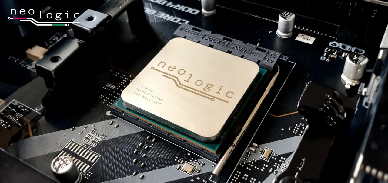
NeoLogic expects to tape out an Arm processor based on its Quasi-CMOS technology, NeoMOS, in a 16-nm process in December, with an eye toward market availability of NeoMOS-based processors in the second half of next year. The processors will aim at delivering high computing power with reduced power consumption and cost for applications such as data centers.
The 2021 Israeli startup, controverting concerns that processor innovation and performance scaling are slowing down, focuses on creating a new path for the semiconductor industry with Quasi-CMOS technology. NeoLogic claims its approach will enable continued reductions in processor real estate and power requirements.
Until now, NeoLogic had only licensed NeoMOS to a select number of companies for integration into their chips, and little information about the technology had been publicly available. But the company now says it has successfully concluded the development phase of Neo-MOS-based standard cells tailored for the 16-nm node and is working toward its next steps.
Quasi-CMOS technology
The development of Quasi-CMOS technology was a result of manufacturers’ efforts to scale down transistor gate length while improving performance. Increasing processing power implies increasing the number of transistors on the processor chip, but the pursuit of size scaling makes circuits crammed and complex. NeoLogic attempts to overcome the downsizing challenge with its novel outlook on processor architecture. The NeoMOS approach integrates single-transistor logic (NMOS or PMOS) with CMOS logic to create logic gates and circuits. The technology reportedly can cut down the number of transistors by three times at any technology node.
“Our design technology enables us to design a 16-nm processor that delivers performance equivalent to more advanced—sub-16-nm—technology nodes while saving development (NRE) (opex) costs,” Avi Messica, co-founder and CEO of NeoLogic, said in a statement.
Data centers are experiencing escalating workloads due to a convergence of factors. The rapid pace of digital transformation across industries, the proliferation of cloud services and the surging prevalence of big data analytics and artificial intelligence applications have led to heightened demands for computational power and data storage. By enabling double-digit savings in power consumption and surface area, Quasi-CMOS technology addresses the complications and increasing burdens of data centers, which are sensitive to power dissipation and seek to maximize computing power per W/mm2.
According to NeoLogic, the reduction in chip size made possible by NeoMOS enables significant savings in semiconductor manufacturing costs. The size reductions lead to improved yield rates, reduced material usage, enhanced production efficiency and lower power consumption. Smaller chips also require less complex packaging and offer higher chip density on a single wafer, leading to cost savings in both manufacturing processes and facilities. Additionally, they can reduce non-recurring engineering costs associated with chip design and testing and lower transportation expenses because of their reduced weight and size. These advantages are particularly valuable at sub-40-nm technology nodes, where costs tend to rise exponentially, allowing semiconductor manufacturers to navigate the challenges of miniaturization while delivering cost-effective and competitive solutions, the company said.
NeoLogic said the NeoMOS technology’s integration of standard CMOS gates and cells with reduced-complexity gates and cells can reduce overall circuit complexity. For example, accommodating six to 32 inputs in CMOS, fan-in–limited (up to four-input) technology, would require a tree topology that would increase the processor’s surface area and power consumption. NeoMOS instead uses six to 32 single-stage gate inputs, reducing critical-path length and enabling the resultant processor to be more compact.
NeoMOS-based cells harmoniously integrate with the existing CMOS standard cell library, according to the company. NeoLogic said its standard cells’ single-stage architecture feature high fan-in capabilities (ranging from eight to 16 inputs) that yield a potential power savings of up to 50% compared with advanced CMOS cells. The cells can also conserve up to 40% of the available area, the company said.
Developing Quasi-CMOS standard cells can be time-consuming relative to CMOS, but Messica asserted that “once the cells are ready, they are seamlessly mixed and matched with standard CMOS cells and have no impact on the design flow.”
The CEO is also confident that NeoLogic can stick to a second-half 2024 timetable for commercial processors based on its technology. Quasi-CMOS cells “are fully compatible with the CMOS fabrication process flow as well as the conventional EDA tools and as such are transparent to the fabs,” Messica said. “Therefore, we do not expect any difficulties in mass production.”
Prospects
The NeoMOS approach reflects the backgrounds and design philosophies of its two co-founders. Messica is an expert in solid-state physics and quantum devices and in ultrafast transistors with 25 years of managerial experience at a variety of tech companies. CTO Ziv Leshem has 24 years of experience in processor design and design project management with companies including National Semiconductor, DSPG and Synopsys. He also co-founded LogixL, which developed a hardware-based HDL simulator, and was a manager at NewSight Imaging, a developer of LiDAR and iTOF sensors.
“NeoLogic has a unique book of knowledge that spans from RTL to chip fabrication,” Messica said. “[We] master the entire process of chip design and fabrication. Leveraging thefabrication capabilities is one of the components of our secret sauce in tandem with the topology modification of circuits and some other tricks.”