Joni Mellin, X-FAB’s product marketing manager responsible for photonics and business development, thinks the project’s timing is right. X-FAB’s foundry has been processing wafers for photonics-related devices across multiple sites in Germany, France and Malaysia for more than a decade, and customer demand for such services is rising—and fast, Mellin said.
“It’s always a little bit of a difficult question, when to start supporting these activities, especially when the market is not yet exactly in place,” he said. “But we’re seeing more and more big companies investing in [integrated photonics] programs, as well as SMEs who have been developing products, now trying to get these into the marketplace.”
Myriad end customers want to develop commercial silicon photonics–related products and are scouting high-volume manufacturing partners, Mellin said. “Integrated photonics has reached a level of maturity where it starts to make sense to install high-volume manufacturing capabilities. The photonics industry had identified this as a roadblock, so we’re working with photonixFAB partners to set up an industrial-value supply chain.”
Integration issues
Photonic integrated circuits (PICs) combine multiple photonic and electronic functions on a single chip to create fast and energy-efficient devices, but blending these wildly different elements onto a chip isn’t easy. Over the past decade, heterogeneous integration methods have been developed to streamline fabrication, but as PICs increase in complexity, such processes have become extremely intricate and not particularly cost-effective.
Given these market developments and to prepare for higher-volume manufacturing, photonixFAB is setting up heterogeneous integration manufacturing lines at X-FAB for silicon-on-insulator (SOI) and silicon nitride (SiN) photonics technologies developed by Belgium-based imec and by Ligentec (Ecublens, Switzerland). In time, the SiN platform will be commercially available through Ligentec.
As part of these activities, components based on indium phosphide (InP), lithium niobate (LNO) and germanium will also be integrated into SOI- and SiN-based PICs. And by the end of the project, each platform will be ready for low-volume production and prototyping at different technology-readiness levels, with a clear pathway in place for high-volume fabrication.
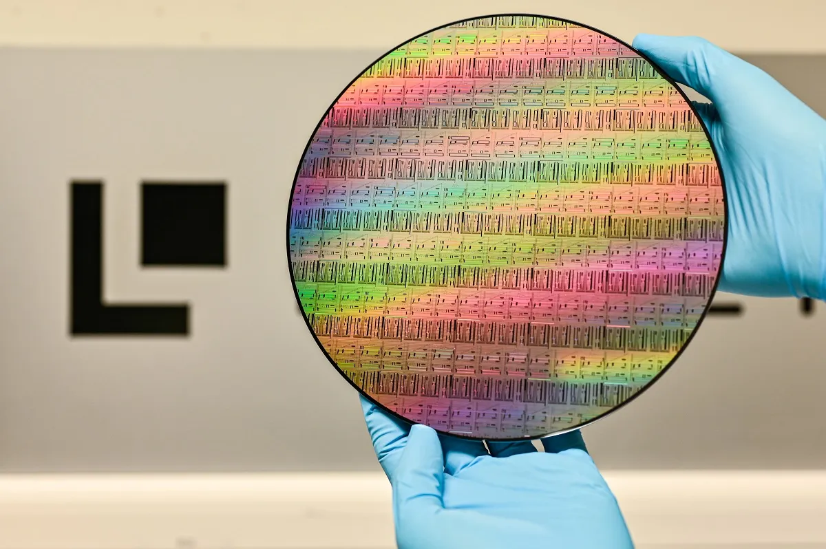
A wafer from photonixFAB project partner Ligentec.
A wafer from photonixFAB project partner Ligentec. The SiN solution pioneer is a spinout of École Polytechnique Fédérale de Lausanne (EPFL). (Source: École Polytechnique Fédérale de Lausanne)
“It’s very difficult to manufacture [PICs] and get high yields, and I understand [companies] are having problems here,” Mellin said. “We need to find a more cost-effective and faster way to make products.” This is where photonixFAB’s processes get interesting.
To date, heterogeneous integration has mostly taken place via die-to-wafer bonding, as well as active alignment of active and passive components. The new project will take a different tack and focus on micro-transfer printing (MTP), as licensed from long-standing X-FAB partner X-Celeprint (Cork, Ireland). According to Mellin, this massively parallel pick-and-place process can stack dies based on different process nodes and technologies to deliver PICs more swiftly and cost-effectively.
“X-Celeprint has been pioneering this [technique], and we have already set up a pilot line for electronic chiplets with them,” he said. “We’re keeping the door open for direct die-to-wafer bonding, but we’re more inclined toward micro-transfer printing right now.”
As part of these activities, X-FAB will also work with photonixFAB partner Smart Photonics (Eindhoven, Netherlands) to streamline the integration of InP components to platforms. Critically, the PIC foundry recently won €100 million in funds from ASML, NXP and other industry and financial investors to ramp up manufacture of InP wafers and chiplets.
“These funds will really help Smart Photonics to scale up future production,” Mellin said. “We intend to combine their InP foundry technologies with our technologies and then provide MTP to [fabricate] devices based on customer designs.”
Along the way, Belgium-based photonic IC design software developer Luceda Photonics will establish mature process design kits for the SOI and SiN technologies and will work with Smart Photonics to enable design for the heterogeneous integration of InP chiplets and LNO materials. Luceda Photonics will also develop PIC assembly design kits to reduce packaging costs, while Phix Photonics Assembly (Enschede, Netherlands) will scale up PIC packaging processes for volume manufacturing. Critically, major application developers Nokia, Nvidia, Aryballe, Brolis Sensor Technology and PhotonFirst are on board to test PICs in use cases like datacom and optical switches and infrared spectrometry for consumer healthcare.
Bold moves
What is clear from the plans laid out by photonixFAB is that the pieces for an industrial-scale integrated photonics supply chain are being carefully put into place—and some might add that it’s about time. It’s no secret that both the U.S. and Asia are a step ahead of Europe on commercial PIC processes. As Mellin put it, “Europe is excellent in investing in basic research, but traditionally, we have not been the ones to successfully commercialize our results.”
The X-FAB product marketing manager noted that European players had been ahead of the pack on semiconductor development, but then manufacturing largely shifted to Asia. “This has perhaps motivated EU decision-makers and member states to provide incentives and programs for a [PIC] industrial value chain in Europe, which is what photonixFAB is all about,” he said. “[With this], our customers won’t need to go to the U.S., China or elsewhere in Asia to get their chips made.”
Indeed, looking beyond the end of the project, Mellin is confident that partnerships will continue to form, enabling the PIC marketplace to flourish. “To benefit from all of our investment here in R&D and basic technology, we have to keep building up our manufacturing base in Europe,” he said. “A lot of people have spent their careers in photonics, and I really hope we are able to meet their commercial expectations and continue to grow.”